All-nitride Superconducting Qubit Made on a Silicon Substrate

- New material platform for large-scale integration of superconducting qubits -

September 20, 2021

National Institute of Information and Communications Technology
National Institute of Advanced Industrial Science and Technology
Nagoya University
Japan Science and Technology Agency

Highlights

  • All-nitride superconducting qubit was realized using niobium nitride with a superconducting transition temperature of 16K.
  • Manufacturing technology on low-loss silicon substrate significantly improves coherence time.
  • Obtained results are expected to be applied to large-scale quantum computers and quantum nodes.

Abstract

Figure 1
Figure 1
(a) Conceptual diagram of microwave cavity and qubit
(b) Optical micrograph of nitride superconducting qubit circuit
(c) Electron micrograph of nitride superconducting qubit (part) and cross-sectional view of the device
(d) Transmission electron micrograph of epitaxially grown nitride Josephson junction
[Click picture to enlarge]
Researchers at the National Institute of Information and Communications Technology (NICT, President: TOKUDA Hideyuki, Ph.D.), in collaboration with researchers at the National Institute of Advanced Industrial Science and Technology (AIST, President: Dr. ISHIMURA Kazuhiko) and the Tokai National Higher Education and Research System Nagoya University (President: Dr. MATSUO Seiichi) have succeeded in developing an all-nitride superconducting qubit using epitaxial growth on a silicon substrate that does not use aluminum as the conductive material. This qubit uses niobium nitride (NbN) with a superconducting transition temperature of 16 K (-257 °C) as the electrode material, and aluminum nitride (AlN) for the insulating layer of the Josephson junction. It is a new type of qubit made of all-nitride materials grown epitaxially on a silicon substrate and free of any amorphous oxides, which are a major noise source. By realizing this new material qubit on a silicon substrate, long coherence times have been obtained: an energy relaxation time (T1) of 16 microseconds and a phase relaxation time (T2) of 22 microseconds as the mean values. This is about 32 times T1 and about 44 times T2 of nitride superconducting qubits grown on a conventional magnesium oxide substrate.
By using niobium nitride as a superconductor, it is possible to construct a superconducting quantum circuit that operates more stably, and it is expected to contribute to the development of quantum computers and quantum nodes as basic elements of quantum computation. We will continue to work on optimizing the circuit structure and fabrication process, and we will proceed with research and development to further extend the coherence time and realize large-scale integration.
These results were published in the British scientific journal "Communications Materials" on September 20, 2021 at 18:00 (Japan standard time).

Background and Challenges

Toward the coming future Society 5.0, there are limits to the performance improvement of semiconductor circuits that have supported the information society so far, and expectations for quantum computers are rising as a new information processing paradigm that breaks through such limits. However, the quantum superposition state, which is indispensable for the operation of a quantum computer, is easily destroyed by various disturbances (noise), and it is necessary to properly eliminate these effects. 
Since superconducting qubits are solid-state elements, they have excellent design flexibility, integration, and scalability, but they are easily affected by various disturbances in their surrounding environment. The challenge is how to extend the coherence time, which is the lifetime of quantum superposition states. Various efforts are being made by research institutes around the world to overcome this problem, and most of them use aluminum (Al) and aluminum oxide film (AlOx) as superconducting qubit materials. However, amorphous aluminum oxide, which is often used as an insulating layer, is a concern as a noise source, and it was essential to study materials that could solve this problem.
As an alternative to aluminum and amorphous aluminum oxide with a superconducting transition temperature TC of 1 K (-272 °C), epitaxially grown niobium nitride (NbN) with a TC of 16 K (-257 °C), NICT has been developing superconducting qubits using NbN / AlN / NbN all-nitride junctions, focusing on aluminum nitride (AlN) as an insulating layer (see Appendix for details).
In order to realize a NbN / AlN / NbN Josephson junction (epitaxial junction) in which the crystal orientation is aligned up to the upper electrode, it was necessary to use a magnesium oxide (MgO) substrate whose crystal lattice constants are relatively close to those of NbN. However, MgO has a large dielectric loss, and the coherence time of the superconducting quantum bit using the NbN / AlN / NbN junction on the MgO substrate was only about 0.5 microseconds [1].

Achievements

Figure 2
Figure 2 Measured coherence times
(a) Energy relaxation time T1=18 microseconds
(b) Phase relaxation time T2=23 microseconds
[Click picture to enlarge]
NICT has succeeded in realizing NbN / AlN / NbN epitaxial Josephson junctions using titanium nitride (TiN) as a buffer layer on a silicon (Si) substrate with a smaller dielectric loss [2]. This time, using this junction fabrication technology, we designed, fabricated, and evaluated a superconducting qubit (see Figure 1) that uses NbN as the electrode material and AlN as the insulating layer of the Josephson junction.
As schematically shown in Figure 1(a), the quantum circuit is fabricated on a silicon substrate so that the microwave cavity and the qubit can be coupled and interact with each other as shown in Figure 1(b). From the transmission measurement of the microwave characteristics of the resonator weakly coupled to the qubit under small thermal fluctuation at the extremely low temperature of 10 mK, we achieved an energy relaxation time (T1) of 18 microseconds and a phase relaxation time (T2) of 23 microseconds. The mean values for 100 measurements are T1=16 microseconds and T2= 22 microseconds. This is an improvement of about 32 times for T1 and about 44 times for T2 compared to the case of superconducting qubits on MgO substrates.
For this result, we did not use conventional aluminum and aluminum oxide for the Josephson junction, which is the heart of superconducting qubits. We have succeeded in developing a nitride superconducting qubit that has a high superconducting critical temperature TC and excellent crystallinity due to epitaxial growth. These two points have great significance. In particular, it is the first time that anyone in the world has succeeded in observing coherence times in the tens of microseconds from nitride superconducting qubits by reducing dielectric loss by epitaxially growing them on a Si substrate. The superconducting qubit of this nitride is still in the early stages of development, and we believe that it is possible to further improve the coherence time by optimizing the design and fabrication process of the qubit.
Using this new material platform that may replace conventional aluminum, we will accelerate research and development of quantum information processing, which will contribute to the realization of more power-saving information processing and the realization of quantum nodes necessary for the construction of safe and secure quantum networks.

Prospects

We plan to work on optimizing the circuit structure and fabrication process with the aim of further extending the coherence time and improving the uniformity of device characteristics in anticipation of future large-scale integration. In this way, we aim to build a new platform for quantum hardware that surpasses the performance of conventional aluminum-based qubits.

Information of the article

Journal: Communications Materials
DOI: 10.1038/s43246-021-00204-4
URL: https://doi.org/10.1038/s43246-021-00204-4

Title: Enhanced coherence of all-nitride superconducting qubit epitaxially grown on silicon substrate
Authors: Sunmi Kim, Hirotaka Terai, Taro Yamashita, Wei Qiu, Tomoko Fuse, Fumiki Yoshihara, Sahel Ashhab, Kunihiro Inomata, Kouichi Semba

Author contributions

All authors contributed extensively to the work presented in this article. S.K., H.T., T.Y., and K.S. designed the experiment and analyzed the data. S.K., W.Q., and H.T. fabricated the samples and characterized the basic junction properties. K.I. performed the microwave measurement. F.Y., T.F., and S.A. supported data analysis. S.K. wrote the manuscript with feedback from all authors. K.S. and H.T. supervised the whole project.

Author affiliations

NICT: Sunmi Kim, Hirotaka Terai, Wei Qiu, Tomoko Fuse, Fumiki Yoshihara, Sahel Ashhab, Kouichi Semba
AIST: Kunihiro Inomata
Nagoya University: Taro Yamashita

Related past press releases

Acknowledgements

This work was partly supported by Japan Science and Technology Agency Core Research for Evolutionary Science and Technology (Grant No. JPMJCR1775), JSPS KAKENHI (JP19H05615), JST ERATO (JPMJER1601), MEXT Quantum Leap Flagship Programs (MEXT Q-LEAP) (Grant No. JPMXS0120319794 and JPMXS0118068682), and the Program for Promoting the Enhancement of Research Universities (Nagoya University).

Appendix

About Nitride Superconducting Qubits

Currently, various attempts are being made by research institutes around the world, including major IT companies such as Google, IBM, and Alibaba, to improve qubit coherence times, but many superconducting qubits use aluminum vapor deposited films. Most superconducting qubits use an aluminum-deposited film as an electrode, and a thin aluminum oxide film on the surface is used as an insulating layer to form a Josephson junction. This amorphous aluminum oxide contains many material defects called two level systems (TLSs), which are known to be an obstacle that hinders the preservation of the quantum superposition state (decoherence). 
The NbN / AlN / NbN junction using niobium nitride (NbN) as the electrode material has the feature of epitaxial growth in which the crystal structure and orientation are all aligned up to the upper electrode, thus there is a possibility to reduce decoherence caused by TLSs. In addition, the superconducting transition temperature TC of aluminum is 1 K, while TC of NbN is as high as 16 K, which means that it is highly resistant to various disturbances (heat and electromagnetic noise entering from the wiring). This means that it is expected to realize a qubit that operates more stably. 
However, the reason why the development of the nitride qubit was delayed despite its excellent characteristics is that the piezoelectricity (piezo characteristic) of the aluminum nitride (AlN) film used as the insulating layer limits the coherence time to about 10 nanoseconds. In order to solve this problem, we focused on the crystal structure of the AlN thin films, and in order to change the crystal structure from the wurtzite showing piezoelectricity to the cubic without piezoelectricity, on a single crystal substrate of the (100) orientation. The epitaxial growth method of NbN / AlN / NbN junction was adopted. Previously, superconducting qubits were evaluated using NbN / AlN / NbN epitaxial junctions grown on MgO substrates, and a coherence time of 0.5 microseconds was observed [1].

Nitride superconducting qubit developed this time

Figure 1 (reuse)

Figure 1 (reuse)
(a) Conceptual diagram of microwave cavity and qubit
(b) Optical micrograph of nitride superconducting qubit circuit
(c) Electron micrograph of nitride superconducting qubit (part) and cross-sectional view of the device
(d) Transmission electron micrograph of epitaxially grown nitride Josephson junction
References
[1] Y. Nakamura, H. Terai, K. Inomata, T. Yamamoto, W. Qiu, and Z. Wang, “Superconducting qubits consisting of epitaxially grown NbN / AlN / NbN Josephson junctions”, Appl. Phys. Lett. 99, 212502 (2011).
[2] K. Makise, H. Terai, and Y. Uzawa, “NbN / AlN / NbN / TiN tunnel junctions on Si (100) substrate for superconducting devices”, IEEE Trans. Appl. Sup. 26, 1100403 (2016). 

Glossary

Superconducting qubit

A type of qubit (the smallest unit of quantum information used in a quantum computer). A qubit realized by a quantum circuit composed of superconductors is a superconducting qubit that can be used to represent a superposition of state |0> and state |1>.

Epitaxial growth

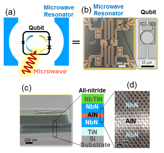
Epitaxial growth is one of the thin film crystal growth techniques. It is a film formation method in which crystal planes are aligned and arranged on a substrate. For epitaxial growth of NbN, a substrate of MgO single crystal having almost the same lattice constant is generally used, but the MgO substrate has a large dielectric loss in the microwave frequency range, so it is not desirable to use it for qubit fabrication. For reference, the lattice constant of MgO is 0.421 nm, and that of NbN is 0.446 nm. In the case of a high-resistance Si substrate, the dielectric loss is an order of magnitude smaller and suitable for qubit fabrication, but its lattice constant (0.542 nm) is significantly different from NbN, so there is a difficulty in epitaxial growth on the Si substrate. However, NICT has developed an epitaxial growth technology for NbN on Si substrates by using TiN (lattice constant 0.424 nm) as a buffer layer between the Si substrate and the NbN thin film, and has made it possible to apply it to qubits.

Niobium nitride (NbN)

One of the materials that develops a superconducting state in which the electrical resistance becomes zero at a temperature below the superconducting transition temperature. The superconducting transition temperatures of niobium (Nb) and niobium nitride (NbN) are approximately 9 K (-264 degrees Celsius) and 16 K (-257 degrees Celsius), respectively. Niobium nitride, which has a high superconducting transition temperature, has the advantage of requiring less power for cooling.

Josephson junction

An element having a structure in which two superconducting electrodes are separated by an ultrathin insulator or a normal conductive metal thin film is called a Josephson element. It can carry an electric current with zero resistance (zero voltage) due to the tunnel effect between the superconducting electrodes. Since the magnitude of this Josephson current is determined by the difference in the macroscopic phase of both superconducting electrodes (DC Josephson effect), conversely, the amount of current flowing through the Josephson element between the superconducting electrodes can be macroscopic. The phase can be controlled. Many superconducting devices such as superconducting qubits are based on the macroscopic phase control by this Josephson element as the basic operating principle.

Amorphous

Must not be crystalline. There is no regularity in the arrangement of atoms and molecules in the solid, and it is also called amorphous substance.

Coherence time

The lifetime of the quantum superposition state. It is the time during which quantum interference continues between two quantum superposition states. When the coherence disappears, the quantum superposition state is lost, and the state of the particles is fixed to one of the states.

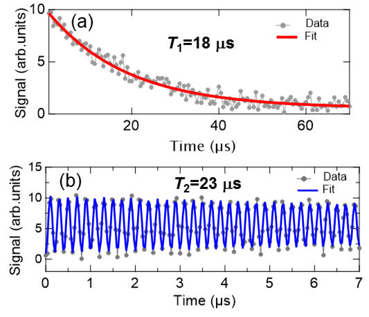
Energy relaxation time (T1) and phase relaxation time (T2)

There are two known qubit coherence times, called energy relaxation time (T1) and phase relaxation time (T2), which characterize the dynamics of a qubit. The energy relaxation time T1 governs how fast the excited state (|1>), which is obtained by irradiating a qubit in the ground state (|0>) with a microwave pulse called a π pulse, releases energy and returns to the ground state |0>. It is a time that represents the process of relaxation. The probability that a qubit is found in the excited state |1> decays exponentially with time, and its time constant is T1. T2 is called phase relaxation time or lateral relaxation time. A microwave pulse called π / 2 pulse prepares the superposition of state |0> and state |1>, and the time until the phase of the superposition state decays with time is called T2.

Quantum node

Long-distance communication of quantum information is made possible by optical fiber optical communication technology, which enables the construction of quantum networks. However, the problem is that the optical signal becomes weaker as the moving distance becomes longer, and the communication speed is limited by quantum noise and so on. In order to solve this problem, quantum nodes allow the quantum properties of optical signals to be freely measured, controlled, and stored at the relay points (nodes) of this network. A quantum node requires a quantum processor composed of many qubits from one qubit depending on the purpose of use.

Society 5.0

The concept of a future society proposed by Japan is a human-centered society that achieves both economic development and solutions to social issues through a system that highly integrates cyber space (virtual space) and physical space (real space).
https://www8.cao.go.jp/cstp/society5_0/

Crystal Orientation

It means that the unit structures (microcrystals) that make up a solid are arranged in a certain direction.

Dielectric loss

When a high-frequency signal (GHz band) is applied to a dielectric, part of the electric field energy of the high-frequency signal is lost due to the thermal energy generated because the phase is delayed from the AC electric field and polarization occurs.

Piezoelectricity

Also called piezo characteristic, when pressure is applied to a certain solid material, it is polarized in proportion to the pressure, and a surface charge appears. Conversely, it also includes the property that a solid material is deformed when an electric field is applied (inverse piezoelectric effect). If a part of the Josephson junction where the electric field is concentrated in the qubit component has piezo characteristics, the coupling between the electric field and the crystal lattice on the substrate side causes energy dissipation on the substrate side due to phonon emission, resulting in fast loss of qubit coherence.

Contact information

Technical Contact

KIM Sunmi, SEMBA Kouichi
Quantum ICT Laboratory
Advanced ICT Research Institute
NICT
Tel: +81-42-327-5684, 7611

TERAI Hirotaka
Superconductive ICT Laboratory
Advanced ICT Research Institute
NICT
Tel: +81-78-969-2191

INOMATA Kunihiro
Research Center for Emerging Computing Technologies
AIST
Tel: +81-29-861-3374

YAMASHITA Taro
Department of Electronic Engineering
Graduate School of Engineering
Nagoya University
Tel: +81-52-789-4425

Media Contact

Press Office
Public Relations Department
NICT
Tel: +81-42-327-6923

Public Relations Department
AIST

Public Relations Office
Nagoya University

Public Relations
Japan Science and Technology Agency